chapter 1: INTRODUCTION
In digital circuit, a shift register is a cascade of flip flops, sharing the same clock, in which the output of each flip-flop is connected to the ‘data’ input of the next flip-flop in the chain, resulting in a circuit that shifts bit by one position the ‘bit array’ stored in it, ‘shifting in’ the data present at its input and ‘shifting out’ the last bit in the array, at each transition of the clock input.
More generally, a shift register may be multidimensional, such that its ‘data in’ and stage outputs are themselves bit arrays: this is implemented simply by running several shift registers of the same bit-length in parallel.
Shift registers can have both parallel and serial inputs and outputs. These are often configured as ‘serial-in, parallel-out’ (SIPO) or as ‘parallel-in, serial-out’ (PISO). There are also types that have both serial and parallel input and types with serial and parallel output. There are also ‘bidirectional’ shift registers which allow shifting in both directions: L→R or R→L. The serial input and last output of a shift register can also be connected to create a ‘circular shift register’.
The final mode of operation is the Parallel-in to Parallel-out Shift Register. This type of shift register also acts as a temporary storage device or as a time delay device similar to the SISO configuration . The data is presented in a parallel format to the parallel input pins PA to PD and then transferred together directly to their respective output pins QA to QD by the same clock pulse. Mode Control input (one clock pulse ) loads and unloads the register.
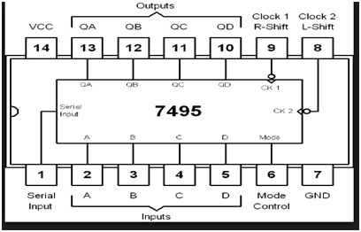
pin diagram of IC-7495
